Table of Contents >> Show >> Hide
- What This PCB Idea Actually Is
- Why Makers and Engineers Are Paying Attention
- What The “Last PCB” Claim Gets Right
- Why It Is Definitely Not The Last PCB You’ll Ever Buy
- How It Compares To The Other Usual Prototyping Options
- Who Should Actually Buy One
- The Verdict
- Bench Experience: What Working This Way Actually Feels Like
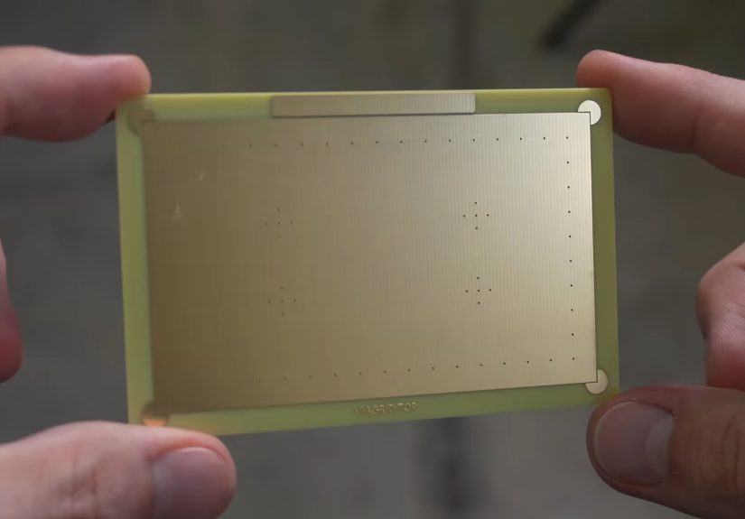
Every so often, electronics prototyping gets a new “this changes everything” moment. Usually, that sentence is followed by a dramatic thumbnail, a laser doing something expensive, and a maker looking like they just discovered fire for the second time. This time, though, the excitement is understandable. The idea behind the question “Is This The Last PCB You’ll Ever Buy?” is genuinely clever: instead of ordering a brand-new custom board every time you tweak a design, what if you stocked a reusable-style prototype PCB platform with factory-made vias already built in and then customized only the copper you needed?
That is the promise behind the recent buzz around via-grid prototype boards, sometimes nicknamed “biscuit boards” or discussed under the name viagrid PCB. The concept is simple enough to explain without a whiteboard and three coffees: buy a standardized blank board with a pre-made grid of plated vias, then use a laser, CNC tool, or similar method to isolate traces and create a working two-layer prototype in-house. In theory, you get the speed of DIY rapid PCB prototyping with one major headache already solved: vias.
So, is this really the last PCB you’ll ever buy? Not literally. Not even close. But it could be one of the smartest PCB purchases you make if your work lives in the sweet spot between messy breadboards and fully custom production boards. The real story is not that one magic board replaces everything. The real story is that modern electronics badly need a better middle ground.
What This PCB Idea Actually Is
To understand why people are excited, it helps to understand the problem it is trying to solve. A traditional breadboard vs PCB decision used to be easy. If you were experimenting, you used a solderless breadboard. If the circuit worked, you moved to perfboard, stripboard, or a custom PCB. Nice and tidy. Very 2008.
Then the electronics world got smaller, denser, and more surface-mount everything. Suddenly the fun little through-hole chip you could toss into a breadboard had a tiny QFN cousin that looked like a grain of rice with trust issues. That is why companies like Adafruit, SparkFun, DigiKey, and SchmartBoard sell so many SMD prototyping aids, breakout boards, and adapter PCBs. They exist because modern parts are powerful, affordable, and often absolutely not breadboard-friendly.
A via-grid board tries to solve that transition problem in a more ambitious way than a simple breakout. Instead of adapting one chip to a 0.1-inch grid, it creates a whole blank prototyping canvas with two layers already connected by a fixed pattern of plated vias. That means you can route signals on top and bottom without drilling and plating every single interconnect yourself. In other words, the board does the annoying part in advance, and you do the creative part later.
Why Makers and Engineers Are Paying Attention
It attacks the real bottleneck
For homebrew PCB work, making a single-layer board is no longer shocking. People mill them, etch them, laser them, and occasionally bully them into existence with pure stubbornness. The hard part is two-layer routing with reliable vias. That is where a via-ready board becomes interesting. It removes the most tedious piece of DIY double-sided PCB fabrication and turns it into an inventory problem instead of a fabrication problem. Buy a stack once, then iterate fast.
It respects the SMD reality
Modern prototyping is no longer a through-hole paradise. A lot of useful sensors, regulators, drivers, and microcontrollers now show up in surface-mount packages first, and sometimes only. That has pushed makers toward adapter boards, breakout boards, and solderable breadboard-style PCBs for years. A viagrid-style approach feels like the next step in that evolution: less “make this one chip usable” and more “make this whole prototype workflow sane again.”
It saves the one thing nobody can buy more of
Time is the strongest argument for the concept. Ordering prototype boards is easier than ever, and U.S. services can be impressively fast. But “fast” in fab-house language still usually means days, not minutes. If you are debugging a motor driver, tuning a power stage, testing a sensor front end, or trying three MCU pinouts before lunch, a tool that lets you go from idea to physical board the same day is not a toy. It is a productivity weapon.
That matters even more in small engineering teams, maker spaces, research labs, and hardware startups. A one-day delay does not sound terrible until it happens six times in one week. Suddenly the calendar is laughing at you.
What The “Last PCB” Claim Gets Right
The headline is exaggerated, but the core insight is strong: many prototype boards are embarrassingly repetitive. Engineers and hobbyists often order one-off PCBs just to validate a small section of a design, test a footprint, confirm connector placement, or route a handful of signals more cleanly than a breadboard allows. In those cases, a standardized prototype board can absolutely replace a large number of disposable quick-turn orders.
That is especially true when the project checks most of these boxes:
- It is a low- to medium-complexity two-layer design.
- It uses common packages and practical routing density.
- It needs plated vias, but not a custom via pattern everywhere.
- It benefits from fast physical iteration more than perfect layout elegance.
- It may eventually become a custom board, but it is not there yet.
For that class of project, a via-grid board is not just useful. It is downright sensible. It lives in the same family as Adafruit’s Perma-Proto boards, SparkFun’s snappable protoboards, and breadboard-layout solderable PCBs, but it pushes the idea into more serious two-layer territory. Think of it as the overachieving cousin who brought plated vias to the potluck.
Why It Is Definitely Not The Last PCB You’ll Ever Buy
Real electrical performance still matters
This is the biggest reason the headline falls apart. Once you care about high-speed digital signals, sensitive analog behavior, RF work, impedance control, return paths, or thermal performance, the physical geometry of the board stops being a detail and becomes the design. At that point, a fixed via grid and a generalized blank board can become a limitation instead of a shortcut.
Breadboards are already notorious for parasitics in faster circuits, which is one reason engineers move to real PCBs in the first place. But even among PCBs, not all layouts are equal. A fabricated custom board validates trace geometry, dielectric behavior, stackup choices, and mechanical tolerances in ways a generalized prototype board simply cannot. If the board layout is part of the product’s performance, then yes, you still need to order the real thing.
Mechanical constraints do not care about your enthusiasm
Sometimes the circuit is easy and the enclosure is the boss. Mounting holes, connector cutouts, edge clearances, antenna keep-outs, daughterboard spacing, thermal zones, and weird product shapes all have opinions. A generic prototype board can help you prove a circuit, but it cannot magically fit inside every product. If your design needs a custom form factor, you are still buying a custom PCB.
Density has a vote too
A fixed via grid is helpful, but it is not infinitely flexible. Fine-pitch BGAs, dense memory routing, specialized power layouts, and anything needing unusual layer planning will hit the limits of the template fast. The board is only “universal” if your project politely agrees to stay within its assumptions. Electronics, unfortunately, are not known for politeness.
Tools and workflow still matter
The via-grid concept makes the most sense if you already have access to the right fabrication tools or a workflow built around them. If you do not own a suitable laser, CNC setup, or assembly equipment, the value proposition changes. A clever board does not eliminate process. It just improves one part of it.
How It Compares To The Other Usual Prototyping Options
Solderless breadboards
Great for learning, quick experiments, and low-frequency circuits. Also great at creating mystery faults after you bump the table with your elbow. Breadboards are still useful, but they are not ideal for dense SMD work, rugged prototypes, or anything sensitive to parasitics.
Perfboard and stripboard
Still valuable, still cheap, still oddly satisfying in a garage-workshop way. Perfboard is the cast-iron skillet of electronics: simple, durable, and a little unforgiving if you do something dumb. But routing can get messy fast, and two-layer sophistication is limited.
Solderable breadboard-layout PCBs
These are excellent when you already proved a circuit on a breadboard and just want a sturdier version without changing the layout. Products like Adafruit Perma-Proto and other breadboard-matching boards are great at this. Their weakness is that they do not fundamentally solve the two-layer routing problem.
Breakout boards and adapters
These are lifesavers for one awkward part. They are not a full board strategy. When your project becomes a colony of adapters perched on jumper wires like tiny metal pigeons, it is time to graduate.
Custom fab prototype PCBs
Still the gold standard for serious validation. U.S. board houses and prototype services can move quickly, and the quality is hard to argue with. If you need real geometry, real manufacturability feedback, and real confidence before production, custom PCB fabrication remains the grown-up answer.
Via-grid or biscuit-style boards
This is the new middle lane. Faster than ordering a new custom board every time, cleaner than a rat’s nest perfboard build, and more capable than a plain solderable breadboard for two-layer work. It is not universal, but it is genuinely useful.
Who Should Actually Buy One
You should seriously consider a via-grid-style PCB prototyping platform if you are a hardware startup doing fast iteration, a lab building functional proofs of concept, a maker space supporting lots of short-cycle experiments, or an advanced hobbyist who regularly outgrows breadboards. It makes sense when you keep making similar classes of boards and can amortize the cost of tools and setup across many builds.
You probably should not treat it as your forever board if your projects are mostly simple through-hole builds, one-off beginner experiments, ultra-dense modern digital systems, RF-heavy layouts, flex designs, or anything headed quickly into production where exact geometry matters more than bench speed.
In plain English: buy it when your bottleneck is iteration, not when your bottleneck is engineering complexity.
The Verdict
So, is this the last PCB you’ll ever buy? No. But it might be the last generic prototype blank you buy for a whole category of projects, and that is still a big deal.
The smartest way to think about this idea is not as a replacement for every custom PCB, but as a replacement for a surprising number of throwaway prototype orders. That is a much more believable claim, and honestly, it is the more exciting one. A tool does not need to be universal to be transformative. It just needs to remove enough friction from a painful workflow that you stop dreading the next revision.
And that is exactly why this concept has legs. It acknowledges the modern reality of SMD parts, the annoying truth about DIY vias, and the constant pressure to move from concept to testable hardware faster. It is not the end of custom PCB manufacturing. It is the beginning of a better in-between.
If your current process is “breadboard, curse, breakout board, curse louder, order PCB, wait, re-order PCB,” then yes, a via-ready prototype board may feel suspiciously close to magic. Not wizard magic, exactly. More like “finally, someone designed a tool for the problem I actually have” magic.
Bench Experience: What Working This Way Actually Feels Like
In real-world prototyping, the appeal of a board like this is less about technical romance and more about emotional survival. The experience usually starts the same way: you have a circuit that is too complicated for a breadboard to stay tidy, but not important enough yet to deserve a full custom fab cycle. Maybe it is a sensor board with a small MCU, a regulator, a connector, and a few passives. Maybe it is a motor-control helper board. Maybe it is a test fixture you swear will only take an afternoon, which is exactly how you know it will consume two days.
On a breadboard, the early version works just enough to trick you into optimism. Then a jumper wire slips. A rail is not actually connected where you thought it was. The tiny surface-mount part you adapted onto a breakout is now attached to the rest of the circuit like a hostage negotiator on a folding chair. The whole build technically functions, but only if nobody breathes near it. This is the stage where you start muttering words that are not suitable for silkscreen.
That is the moment a via-ready prototype board starts to make emotional sense. Instead of treating every revision like a fresh manufacturing event, you start treating the board as bench stock. You pull one from the shelf the way a woodworker grabs a sheet good or a machinist grabs bar stock. The blank is already smart. It already solved the annoying inter-layer problem. You are no longer beginning from raw fiberglass and wishful thinking; you are beginning from a platform.
The workflow also feels different in a practical way. You stop asking, “Is this revision worthy of sending out?” and start asking, “Is this revision worth testing right now?” That is a healthier question. It encourages more iteration, smaller risks, and faster learning. You can test a power-entry section today, revise a connector footprint after lunch, and rework a signal path before the day is over. Even when the result is ugly, it is productive ugly. It teaches you something immediately.
There is also a confidence shift that comes from holding a physically solid board instead of a fragile temporary setup. Soldered joints behave. Connectors stay put. The circuit becomes something you can probe, rework, hand to a teammate, and plug in again tomorrow without rebuilding half of it. That stability changes your thinking. You debug more systematically. You take measurements with less suspicion. You spend less time proving the prototype exists and more time learning whether the design is good.
Of course, the experience is not perfect. The board will occasionally remind you that it is a compromise. A via is never exactly where you want it. A dense section wants a cleaner custom layout. A mechanically awkward connector placement makes you wish you had already ordered the final board. That is fine. Those moments are not proof the concept failed. They are proof you have reached the point where the project deserves something more specialized.
And that is probably the most honest experience of all: a board like this does not eliminate the journey from prototype to production. It simply makes the messy middle far less painful. In electronics, that is not a small victory. That is half the battle.